 |
|
Contact Description
Office: MEYR 366
Phone: 410-455-3427
Email: singna@umbc.edu
|
Research Professor
Post-Doctoral Rensselaer Polytechnic Institute, Troy, NY 1979; Ph.D. Gorakhpur University, India 1977
Professional Interests
Dr. N. B. Singh, a Research Professor in the Department of Chemistry and Biochemistry, and Department of Computer Science and Electrical Engineering is a Fellow of the American Society of Materials (ASM) International, a Fellow of the Society of Photonics and Instrumentations Engineering (SPIE), a Fellow of the Optical Society of America and a Fellow of the Royal Society of Chemistry (RSC). He is internationally known for his researches on Electronic, EO, Lasers, AO, RF materials, and Chemical, Biological and Radiation detectors and sensors. Dr. Singh’s interests center on “Development of Materials, Devices and Subcomponents for Military and Commercial Applications” which utilize solidification, physical vapor transport, crystal growth of bulk, thin crystals, nanoengineered materials, multi-layered coatings, device fabrications and characterization. Currently, this research has following foci:
1. Multifunctional electronic, EO, RF and radiation sensor materials and processes: Development of chemical and mechanical processes which involved
chemistry, thermodynamics, fluid flow, etching, coatings and metallurgical knowledge.
2. Hydroxyapatites for bone and laser host materials for high power lasers: Several halides and SiC-AlN has very high thermal conductivity compared to commercial YAG host and can be used for high power lasers. We are developing novel method and composition for high IRCM power applications.
3. Dielectric materials with colossal values for high pulse power: Development of materials with dielectric constant greater than100, 000 and processes to meet the requirements of high energy pulse applications.
4. Radiation detector materials: Development of novel class of detectors such as halides and chalcogenides for for radiation detections and organic and organometallic molecules for neutron detection.
5. Nanoengineered materials for high temperature operating SWIR and MWIR detectors: Nanocubes and nanodots of PbSe, PbS and solid solution materials which have great potential for the high temperature detectors.
6. Nanowires based Naño-APDS and Nanoelectronics: Nano-APDs for single photon detections and nanoelectronic for high frequency and low power applications.
7. Novel large area substrates materials for Commercial/Defense Applications: large area (6”) size SiC is essential for commercial and defense applications. Physical vapor deposition (PVD) cannot produce at this stage high quality large size boules of that size.
8. SiC–AlN Wurtzite materials for commercial and defense Electronics: GaN is a hexagonal material and requires hexagonal substrates.
9. AOTF based Hyperspectral Imagers: Practical Mid wave infrared (MWIR) and long wave infrared (LWIR) multi/hyperspectral Acousto-Optic (AO) crystal based imagers using unique and very anisotropic crystals grown by Bridgman and PVD method.
10. NLO materials for MWIR and LWIR Laser development: Practical Second harmonic (SHG) and Optical Parametric Oscillation (OPO) laser materials and fabricate by using all common mode of solidification encountered in casting, welding processes and crystal growth. Effort is focused to produce materials for lasers, Missile warning systems, AO based hyperspectral imaging and all electronic beam deflectors.
11. UV Filter Sensors for missile warning: UV Sensors for missile defense applications for military and commercial aircrafts using crystallization method.
12. Eutectic, monotectic and dendritic alloys: Solidification behavior of eutectic, monotectic and dendritic alloys for structural applications.
13. Novel approach for Diamond-Al and Diamond-Cu Heat spreader: Developed a novel approach to process materials which produces high conductivity.
14. Microstructure evolution in annealed multi-phase alloys to generate Capacitor and Railgun Materials: Quantitative description of microstructures
constitutes the core of this research focus, using stereology and metallography combined with modern image analysis.
15. Heterostructure materials for high power RF applications: Wide band heterostructures of SiC and AlN by PVD for high power applications: Interactions
involve fluid-mechanical forces, convective heat transfer, and solutal diffusion fields near solid-liquid and solid-vapor interfaces.
16. Coating developments (AR, AT and Protective): Coatings for anti-reflection (AR), anti-tamper (AT) and protection applications: Involves design and multi-level coatings for wafer, devices and components.
17. Nano-Engineered quantum dot limiters for laser threat: Surface Plasmon Polaritons Quantum Dot Limiters (SPPs-QDTL) for laser threat using quantum dots.
18. Focal Plane materials and IR detectors: CdZnTe and high temperature FPA materials such as PbSnTe class of materials. 7” diameter CZT for MCT substrates using unique approach of Northrop Grumman Corporation.
19. MWIR and LWIR Lasers-QPM: Quasiphase materials for Laser IRCM and imaging, EM and Structural applications; Involves domain engineering, bandgap engineering for EO applications and lattice hardening for structural applications.
20. Organic materials for large area substrates and high efficiency frequency conversion applications: Organics materials are low cost options for substrates and
excellent frequency conversion materials for short wavelength infrared (SWIR).
Selected Publications
A list of the publications, presentations and internal reports is given here. Dr. Singh has published more than 200 journal papers in highly reputed international journals, and more than 120 papers in conference, presented more than 110 invited and plenary lectures. He has written more than 220 trade secrets
including 23 patents. He has been in editorial board of several journals and currently he is an Associate Editor of the journal Progress in Crystal Growth and Characterization
- N. B. Singh, Christopher Cooper, Pietro Strobbia, Narasimha Prasad, Ching Hua Su, Bradley Arnold, Fow-Sen Choa, “Nanomorphology and performance of pure and doped lead selenide for infrared detector; Opt. Eng. 56(7), 077106 (2017)
- N. B. Singh, Ching Hua Su, Bradley Arnold and Fow-Sen Choa, Stacey Sova and Christopher Cooper, “Multifunctional 2D-materials”, J. Materials Today 4, 4 5478-5487 (2017).
- N. B. Singh, Ching Hua Su, Bradley Arnold and Fow-Sen Choa, ”Optical and morphological characteristics of ZnS-ZnSe solid solution” Optical Materials 60, 474-480 (2016)
- N. B. Singh, Ching Hua Su, Bradley Arnold, Fow-Sen Choa and Teja Nagordona, “Low gradient growth of Tl 3 AsSe 3 ” crystals, J. Optical Engineering, 60, 81-85 (2016).
- Puja Gautam, Ankur Khare, Sunita Sharma, N. B. Singh and K. D. Mandal, “Characterization of Bi 2/3 Cu 3 Ti 4 O 12 ceramic synthesized by semi wet route” Natural Science: Materials International, 26, 6 567-571 (2016).
- S. Sharma, M. M Singh, N. B Singh and K. D. Mandal “Processing, properties and design of advanced ceramic composite, Ceramic Transaction, 259,117-131 (2016)
- Shiva S. Yadava, Laxman Singh, Sunita Sharma, K.D. Mandal, “Effect of temperature on dielectric and ferroelectric properties of nanocrystalline hexagonal Ba 4 YMn 4 O 11+δ ceramic synthesized by chemical route”, Royal Society Chemistry Advances, 6, 68247-68253 (2016).
- Laxman Singh, U. S. Rai, K D. Mandal and N. B Singh, “Progress in perovskite functional dielectric material CaCu 3 Ti 4 O 12 ”, J. Progress in Crystal Growth and Characterization, 60, 15-62 (2014).
- U.S.Rai, Laxman Singh, K D. Mandal and N. B Singh, “ An Overview on Recent Developments in the Synthesis, Characterization and Properties of High Dielectric Constant Calcium Copper Titanate Nano-Particles” Journal of Nanoscience and Technology, 1, (1)1-17 (2014).
- N. B Singh, S. R Coriell, Matthew King, Brian Wagner, David Kahler, David Knuteson, Andre Berghman and Sean McLaughlin, Growth Mechanism and Characteristics of Semiconductor Nanowires for Photonic Devices”, Journal of Nanoscience and Technology, 1 (2) 1-8 (2014).
- Narsingh B. Singh. Margaret Gillan, David House, Ravali Yanamaddi, Vishnu Razdan and Bradley Arnold “Effect of substitution and impurities on dielectric properties and resistivity of CaCu 3 Ti 4 O 12 ” J. Emerging Materials Research 2, 6, 344-347 (2013)
- N. B. Singh, A. Berghmans, M. King, D. Knuteson, J. Talvacchio, D. Kahler, M. House ,, B. Schreib, B. Wagner, S. McLaughlin, “Modification of interface anisotropy and its effect on microstructural evolution during ostwald ripening” Crystal Research and Technology, 18, 11, 983-988 (2013).
- N. B. Singh, David House and Bradley Arnold, Novel IR Detector Materials: Hyperstructure and meta morphology formation in heavy metal Chalcogenides, Journal of Advance Materials Manufacturing and Characterization, 3, 1, 2, 15-19 (2013)
- N. B. Singh, A Berghmans, D. Knuteson, J. Talvacchio, D. Kahler, M House, B. Schreib, B. Wagner and M. King, Evolution of microstructure due additives and processing, Ceramic Transaction, 235, 65-76 (2012).
- N. B. Singh et al, Selenides for Nonlinear applications, J. Emerging Materials Research , 1, 185-200 (2012)
- N. B. Singh et al, Performance of Novel Materials for Radiation Detection: Tl3AsSe3, TlGaSe2, Tl4HgI6, J. Nuclear Instrumentation and Methods in Physics Research Section A 652, 183-185 (2011)
- N. B. Singh et al, Characteristics of thick ZnSe films on quasi-phase- matched (QPM) GaAs substrates”, J. Crystal Growth, 312, 1142-1145 (2010)
- N. B. Singh et al, Quaternary AgGaGe n Se2 (n+1) crystals for NLO applications, J. Crystal Growth 312 , 1114 (2010).
- N. B. Singh et al, Effect of AlN doping on the growth morphology of SiC, J. Crystal Research and Technology, 44, 9 903-909 (2009)
- N. B. Singh et al, Optical probes of orientation patterned ZnSe quasi-phase- matched devices, J. Optical Engineering , 48(11), 114201 (2009).
- N. B. Singh et al, (SiC) x (AlN) 1-x solid-solution substrates for high temperature and high power devices, Crystal Growth and Design, 10 (8), (2010) 3508–3514
- N. B. Singh et al, AOTF materials for hyperspectral imagers, Advanced Materials and Processes, September, 31-33 (2010).
- Effect of growth parameters on the morphology and resistivity of PbSe, J. Crystal Growth, 311, 1080- 1086 (2009)
- N. B. Singh et al, Novel quaternary semiconductor materials; growth and characterization, IEEE Trans. Nuclear Sci. 56, 3 813 (2009).
- N. B. Singh et al, Development of Advanced Radiation Materials and Sensors, ES Technical Journal, 1, 4, 53-64 (2008).
- N. B. Singh et al, Morphology of thick SiC epitaxial film grown by PVT method, J. Electronic Materials 37 (2008) 379.
- N. B. Singh et al, Operational characteristics of LWIR AOTF based multispectral imager, J. Optical Engineering Vol.47, 1, 013201 (2008).
- N. B. Singh et al, Crystal growth, fabrication, and design of mercurous bromide acousto-optic tunable filters; Optical Engineering, 46, 6, 064001-6 (2007).
- N. B. Singh et al, Properties of NLO Crystals in THz Wavelength Region, J. Optical Engineering, 45(9), 094002-1 (2006).
- N. B. Singh et al, Periodically Poled Materials for Long Wavelength Infrared (LWIR) NLO Applications, J. Crystal Growth, 274/1-2, 132-137 (2005).
- N. B. Singh et al, X-ray studies of langasite film grown by LPE, J. Materials Science Letters, 22, 1621 (2003)
- N. B. Singh et al, Noncollinear optical parametric oscillator design for walk-off reduction in GaSe crystals, Opical Engineering 42/11, 3270(2003)
- N. B. Singh et al, Physical vapor transport growth of large AlN crystals, J. Crystal Growth 250/1-2, 107(2003)
- N. B. Singh et al, PVT growth and characteristics of AlN single crystals, Physics of Semiconductor Devices 1, 117 (2003)
- N. B. Singh et al, Microgravity experiment to understand the effect of convection on PVT crystal growth Adv. Space Res. 32, 211 (2003)
- N. B. Singh et al, Solutal convection during growth of organic NLO crystals, Progress in Crystal Growth and Characterization, 44, 3 169 (2002).
- N. B. Singh et al, LPE Growth of langasite film for resonator and oscillators, J. Crystal growth, 234, 660 (2002)
- N. B. Singh et al, GaSe: A novel and efficient NLO crystal for mid- and far-IR wavelength, Encyclopedia of Materials Science and Technology, 3463, (2001).
- N. B. Singh et al, Measurement of thermal conductivities in lead bromide, J. Crystal Growth, 225, 512 (2001)
- N. B. Singh et al, Growth of vanillin crystals for second harmonic generation (SHG) applications in the near-IR wavelength region, J. Crystal Growth, 225, 470 (2001)
- N. B. Singh et al, Performance of TAS crystal for AOTF imaging, J. Crystal Growth, 225, 124 (2001)
Honors and Awards
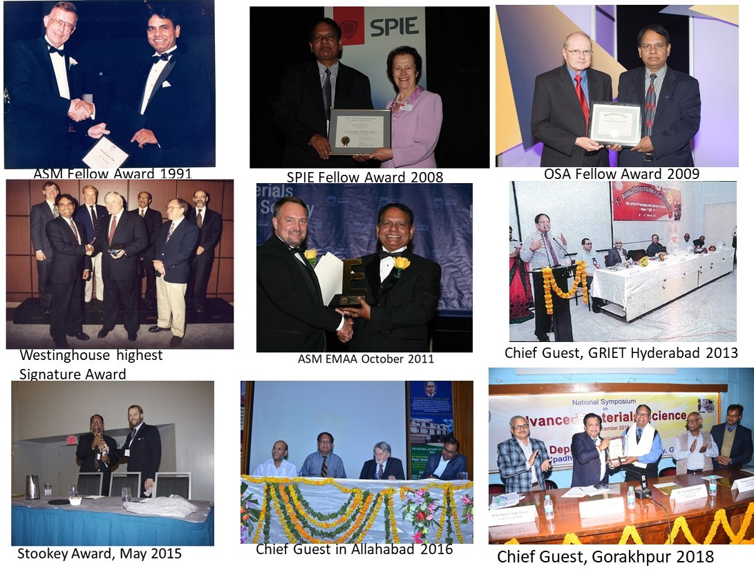
Dr. Singh has been honored with more than thirty national and international awards including;
- Stookey Award of the ACeS Glass & Optical Materials Division and the Deutsche Glastechnische Gesellschaft (GOMD-DGG) for innovation, and life time contribution 2015
- Gold Medal Award of Indian Association of Solid State Sciences and Allied Researchers “Life time contribution” ICFM 2015, Nagpur India 2015
- Fellow, Royal Society of Chemistry “Multidisciplinary Materials and Device Research”, 2014
- Fellow Optical Society of America for “Growth Design and Development of Novel Crystal Based Devices” 2010
- Engineering Materials Achievement Award of ASM International “For the Development of Material for an AOTF (Acousto-Optic Tunable Filter) based Hyperspectral Imager for Homeland Defense Applications.” 2010
- Fellow, ASM International for development of “Heavy-Metal Halides for Opto- electronic Devices” 1991
- Fellow, SPIE-The International Society for Optical Engineering for the development of “High Temperature UV Filters for PMAWS”.2008
- Industry Week R&D Star Award (Worldwide) in 1995
- Westinghouse Corporate Wide Signature Award on Development of Crystals for PMAWS by President of the Westinghouse Electric Corporation 1995
- American Society of Materials-Indian Institute of Metals Lectureship Award, 2013
- Optical Society Lectureship Award 2012.
- Outstanding of the 20 th Century, International Biography Center, Cambridge, UK, 1999
- International Advisory Board member, International Conference on Science and engineering of materials, Noida, India January 2014.
- International Advisory Board member, International Conference on futuristic materials and emerging trends in forensic and life sciences, Nagpur, India Feb. 2015 and engineering of materials, Noida, India January 2014.
- International Advisory Board member, International Conference on Fiber optics and Photonics, Guwahati, India, 2011
- Associate Editor, Journal of Progress in Crystal Growth and Characterization, Elsevier Press 1994-Present
- Honorable Mention for “Effect of anisotropy during Ostwald ripening”, Metallographic Society, 2011
- Advisory Board of HBCU-RISE NSF Center, Alabama A&M University, 2008
- Smt. Mayawati Juneja Award, Life time achievements from Indian Association of Solid-State Chemists., 2005
- Certificate of recognition for completing ES University, President Northrop Grumman ES, 2003
- Advisory Board, Center of NLO Materials, Alabama A&M University 2002-2005
- ASM-IIM Lectureship Award, American Society of Materials 2003, 2013
- National Academy of Engineering Panel Member, Committee on Materials Research for Defense, National Materials Advisory Board, , 2001-2005
- Saul Award, for outstanding teacher and researchers, Prasad Institute, Jaunpur India, 2006
- Distinguished Student list of the University, (Chemistry), Gorakhpur University, India 2002
- Certificate for contribution and outstanding services, The Metals, Minerals and Materials Society (TMS) 1999
- Certificate for contribution to Chemistry, Pittsburgh Chemists Club 1995
- Award for recognition and contribution as the Chair of Gordon Conference on Physio-Chemical Processes”, Chairman, board of trustee, Gordon Conferences 1993.
- Certificate for contribution and outstanding services, The Metals, Minerals and Materials Society (TMS) 1993
- Advisory Board International Conference on Crystal Growth (1990, 1993)
- Mid-Atlantic Section Crystal Growth Award, Mid Atlantic Section of American Association for Crystal Growth, 1991
- Senior Crystal Growth Award, Pittsburgh Chapter of AACG 1992
- Member of Editorial Board, International Materials Reviews ( 1993 served three years)
- Certificate of creative investigation on a research paper by NASA.
- Award for the services and contribution by electronic materials Committee of ASM, American Society of Materials 1986
- Honorable mention by International Metallographic Society on “Effect of anisotropy on dendritic morphology”;1983
- Honor by Director, Westinghouse Solid-State Sciences Division for the improvement of TAS crystals, 1985.
- COSIP award of UGC on Zone-melting Studies of Eutectics, Gorakhpur University UP, India, 1974
Referee
For more than 30 journals including;
- Journal of Crystal Growth
- Journal of Optical Materials
- Molecular Crystal and Liquid Crystals
- Indian Journal of Chemistry
- Indian Journal of Pure and Applied Physics
- Journal of Materials Science and Engineering
- Journal of Chemical Thermodynamics
- Journal of Emerging Materials Science
- Met Transactions
- Journal of Chemical Engineering
- Journal of Optical Engineering
- Journal of Crystal Design
- Journal of Crystal Research and Technology
- Journal of American Chemical Society
- Journal of Optical Society of America
Panel member, Several Awards Committee
- ACeS, ASM, OSA 2011-Present
- International Advisory Committee member Indo-US Workshop on Spectroscopy, 2013
- International Advisory Board of the Meeting
- International Conference on Multifunctional Materials, Energy and Atmosphere, Sharda University, India, August 2013
- ASM International-Indian Institute of Materials Visiting Lectureship Award
- American Society of Materials (ASM) International and Indian Institute of Materials Joint Award, Octobet 28, 2013
Meetings/Events
- Organizer and Chair, “Multifunctional materials for EO, Electronic and Rad Sensors,Materials Science and Technology -17”, Pittsburgh, PA 2017.
- International Conference on Multifunctional Materials, Patna, UP, India, October 2016
- International Conference on Applied and Multifunctional Materials, BHU, Varanasi, India, October 2015
- National conference of Chemists and allied researchers, Delhi, India, May 2015
- International Conference on Multifunctional Materials, Energy and Atmosphere Sharda University, Noida, India , August 21-23, 2013
- MST-13: Joint meeting of American Society of Materials, American Ceramic Society, The Mineral and Materials Society and Iron and Steel Society, Columbus, October 27-31, 2015
- MST-13: Joint meeting of American Society of Materials, American Ceramic Society, The Mineral and Materials Society and Iron and Steel Society, Montreal Canada, October 27-31, 2013
- OSA Fellow Lectures 2013
- Sharda University, Noida (UP) India
- Banaras Hindu University, Varanasi (UP) India
- BBS Purvanchal University, Jaunpur (UP) India
- Tilak Dhari Post-Graduate College, Jaunpur (UP) India MST-17, October 8-12 2017 The main thrust of the workshop is to explore and analyze and view in deep the cutting edge researches in multifunctional materials for EO, electronic, RF and radiation sensors.
- SPIE -Photonics and Optics, San Diego, CA , 2015, 2017 Invited Speaker
- MST-: Joint meeting of American Society of Materials, American Ceramic Society, The Mineral and Materials Society and Iron and Steel Society, Pittsburgh, PA, October 7-11, 2012-2017
Organizer and Chair
ASM-IIM Lectures 2013
- IIT, Banaras Hindu University August 17, 2013
- Udai Pratap Post Graduate College, Varanasi, August 12, 2013.
- International Conference on Multi-functional Materials, Sharda University, August 21-23, 2013
Research Description
Dr. Singh and his group is involved in materials research and technology development which is focused on designing, modelling, growth and fabrication and coating (EO) materials for detectors, RF materials for high power RF and electronics, and materials for radiation detectors. He has personally performed and managed research for many development programs for bulk and nano engineered, FPA materials such as CZT and most recently Si based substrates for MCT substrates and CZT for radiation detection, acousto-optic (AO) based sensors, dielectric materials, QPM structures for Mid-IR lasers and AlN and SiC substrates for high power RF and high temperature microelectronics, organic materials for substrates and nonlinear optical (NLO) applications and radiation detector materials. He has transferred AO sensor technologies using TAS, high temperature UV filter for PMAWS system, and hyperspectral imaging technology based on TAS crystals for far-IR wavelength.
His researches can be summarized as:
- Nanoengineered cubes, rods and dots for SWIR and MWIR detectors
- Chemical and materials processes for sensors
- Dielectric Materials with colossal values for high pulse power
- Hydroxyapatites for bone and Laser host materials for Lasers
- Nano-Engineered Quantum Dot limiters for Laser threat
- Radiation Detectors and Materials
- AOTF based Hyperspectral Imagers
- Nanowires based Naño-APDS
- NLO Materials for MWIR and LWIR Laser Development
- Novel approach for Diamond-Al and Diamond-Cu Heat spreader
- SiC Bulk single crystals and novel large area materials for Commercial/Defense Applications
- UV Filter Sensors for Missile Warning
- Large bandgap materials such as Ga 2 O 3 and SiC –AlN Wurtzite materials for Commercial and Defense Electronics
- Focal Plane Materials and IR detectors
- MWIR and LWIR Lasers
- Organic Materials for Substrates and high efficiency NLO Applications